
Essential PCB Panelization and Thermal Design Strategies for Reliable Board Performance
In modern electronics, Printed Circuit Boards (PCBs) serve as the foundational platform for mounting and connecting components. For high-quality PCB production and reliable performance, two aspects are critical—panelization and thermal design. These design phases not only impact product performance but also determine production cost, assembly efficiency, and longevity.
At PCBYES, with more than 5 years of experience in PCB prototype and fabrication, we are committed to meeting the needs of customers with expert PCB design, manufacturing precision, and outstanding PCBA turnkey services. In this article, we explore key guidelines on how to panelize PCBs for SMT assembly and the thermal design to help engineers and designers ensure optimal functionality and cost-effective mass production.
PCB Panelization Standards You Should Know
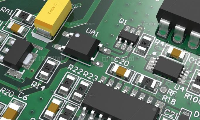
PCB panelization refers to grouping multiple smaller boards into a single larger panel, which streamlines the SMT assembly process, reduces handling errors, and improves manufacturing throughput.
1. Optimal Panel Dimensions
- Maximum panel width should be:
- ≤260mm for SIEMENS SMT lines
- ≤300mm for FUJI SMT lines
- For automated gluing processes: ≤125mm × 180mm
- Square-like shapes such as 2×2 or 3×3 grids are preferred for a balanced panel layout.
2. Mechanical Design of the Panel Frame
- Use a closed-loop frame to prevent deformation during fixture clamping.
- Maintain sub-board center spacing between 75mm and 145mm.
- Avoid placing bulky components near V-cuts or routing bridges.
- Ensure at least 0.5mm of edge clearance around components to avoid interference with cutting tools.
3. Tooling Holes and Fiducial Marks
- Each panel should have 4 positioning holes (Ø4mm ± 0.01mm) with smooth walls and precise placement.
- Every individual board should feature at least 3 tooling holes (3–6mm diameter), with no traces or pads within 1mm.
- Use paired fiducial marks placed diagonally on sub-boards, especially for QFPs with pitch < 0.65mm.
- Leave a 1.5mm solder mask clearance around fiducial marks for better recognition.
4. Component Layout Considerations
- Avoid placing I/O ports, microphones, switches, or batteries near tab routes.
- Large components should include positioning holes or pillars to improve stability during assembly.
At PCBYES, our engineers strictly follow these industry-aligned panelization guidelines to ensure efficient production and outstanding board integrity for every project.
PCB Thermal Design – Why It Matters and How to Optimize It
As device performance increases, so does power consumption and thermal output. Effective thermal design is essential to maintaining product reliability, especially in high-density or power-critical applications like RF, FPGA, or power supply modules.
1. Why Thermal Design Is Crucial
- Heat buildup can result in:
- Component failure due to overheating
- Shortened product lifespan
- Reduced overall system reliability
With modern SMT techniques increasing component density and reducing board area, thermal management has become more important than ever.
2. Thermal-Aware Component Placement
- Place temperature-sensitive components (excluding sensors) near the air inlet, upstream of heat sources.
- Place high-heat-tolerant components (e.g., MOSFETs, power ICs) near air outlets or board tops.
- Space out heat-generating components to prevent thermal clustering.
- Align tall components behind shorter ones in the direction of airflow to avoid blocking convection.
- Orient components along the path of least airflow resistance.
3. Heatsink and Airflow Optimization
- For natural convection, align heatsink fins vertically.
- For forced airflow systems, align the fins with the airflow direction.
- Avoid closely stacking heatsinks along airflow paths—this leads to poor airflow to downstream components.
- Staggered heatsink layout or offset fins for better cooling performance.
- Maintain spacing from other parts based on thermal radiation calculations.
4. Leveraging the PCB as a Heat Sink
- Use thermal vias to conduct heat from components to inner plane layers.
- Utilize wide copper pours (preferably exposed through solder mask windows) to act as large-area heat spreaders.
- Consider ground planes or thermal pads under power ICs for efficient dissipation.
From schematic placement to layout routing, thermal management should be integrated at every step of PCB design. A good thermal strategy ensures that the board remains within safe operating temperatures and extends the life of electronic components.
With our skilled engineering team and full-service PCBA capabilities, PCBYES is your reliable partner in creating thermally optimized and assembly-ready PCB solutions that meet the demands of today’s electronics market.
PCB panelization and passive thermal management in PCB design are two foundational pillars of successful electronic product development. By following proven standards and integrating effective heat management techniques, designers can avoid costly production issues, extend product life, and ensure consistent quality.
Whether you’re prototyping or preparing for mass production, PCBYES delivers excellence in every board we manufacture. Contact us today to learn how our advanced capabilities can bring your designs to life with precision, speed, and reliability.


